Panelizing a KiCad design for DirtyPCBs

@TomKeddie has already recorded useful information on panelizing for DirtyPCBs but as I don’t use Eagle or Windows, I need to work out a different process. And since I don’t have my own blog, you all get to hear about it. Lucky you?

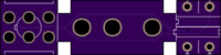
Rather than getting a bunch of different designs built, I had one small design, and I wanted a lot of them. Here’s an OshPark prototype:

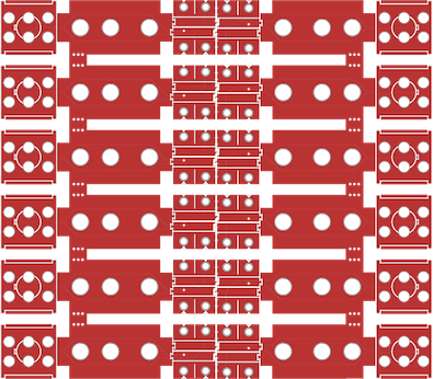
This is 50x12.5mm. In theory, I could fit 16 of them on a 10x10cm prototype board in an 8x2 grid, but that seemed a bit tight; I didn’t want to specify mouse bite holes along the entire long edge of the board, or use Dirty’s “maybe, maybe not” v-groove capabilities. And Dirty produces around 10 of these 10x10cm boards per order - I don’t need that many, do I? After some playing around I settled for 6x2 boards. The end result looks like this:

What I want to document is how I got from OshPurple singles to that DirtyRed panel, because I find online documentation to be surprisingly sparse on the subject.

The main tool I settled on is a Python script called KiCad Panelize. The way you use this is to gather one or more PCB layouts that you want to panelize, create a configuration script that describes how to build your panel from your source PCB layout(s) and run panelize.py to create a new KiCad PCB file with your combined designs.

Here’s my config file to convert from the purple board to the red one:

new
load 'single.kicad_pcb'
source-area 145 111 195 126

copy 120  40
copy 120  55
copy 120  70
copy 120  85
copy 120 100
copy 120 115

rotate-180 170  37.5
rotate-180 170  52.5
rotate-180 170  67.5
rotate-180 170  82.5
rotate-180 170  97.5
rotate-180 170 112.5

save panelize.kicad_pcb

Yes, that took a few tries to get right, but iterating was quick and easy. The obvious question is where did the tabs and mouse bites come from? I cheated, and tweaked my original KiCad design:

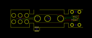
A bunch of stuff is hidden there for clarity, but the key point is that I modified the board outline so that when pasted together by panelize.py, everything fits together. I just needed to fix the outline at four points at the edge of the panel (two extra tabs and two gaps) and add another single row of mouse bites down the middle of the panel.

That gets me a design that’s almost ready for uploading to DirtyPCBs, but there were a few steps left. I’ll document that in a bit. Also I have the boards now and they look okay from outside the packaging, but I haven’t started de-panelizing them. I’ll be trying that tomorrow, and hopefully I’ll be able to report back success… fingers crossed.

5 Likes

Thank you for posting this. I am also working on some PCB’s on Kicad that I want to order, and I was myself wondering about panelization. This will be my first time ordering custom PCB, and I’m going for a 10x10cm panel not from DirtyPCB but from Elecrow.

I’ll probably go for those V-grooves on mine, maybe in combination with some holes at the corners. But I’ll have to figure out their design rules.
On the “Panelizing” section on this page they have options for “X number different sub-PCBs” which cost extra. Does this mean how many separate PCB’s are etched together on the same board? But on this special deal which I’m ordering from the only options are for extra “copies”. :confused: I’ll probably email them to clarify what they mean. It might be just bad English, given they’re located in China.

1 Like

I find those PCB order forms so confusing. All I can guess is that they charge extra to take one or more designs from you and build a panel themselves. If that’s the case, my panelized file that I sent to DirtyPCBs would count as a “Single PCB with milling”, but if I sent the board house just the original 50x12.5mm design and they created that panel, they’d charge it as “11-30 copies + $16”. But I could be totally wrong about that. If you get a clear answer, please document it for the rest of us!

On with the DirtyPCBs ordering notes.

Once you zip up your gerbers and upload them, Dirty gives you two diagnostic tools to help ensure your order will go through. First is a set of renderings of the top and bottom of the board and each individual gerber:

The second is their ‘Layer Report’, which primarily tells you what they think each gerber layer is for. My renderings looked as expected, but I had some issues with this report. By default, KiCad generates file names that look like this:

my_project-B.Cu.gbr
my_project-B.Mask.gbr
my_project-B.SilkS.gbr
my_project-Edge.Cuts.gbr
my_project-F.Cu.gbr
my_project-F.Mask.gbr
my_project-F.SilkS.gbr
my_project.drl

That is, everything is a .gbr file except for the drill file. The renderer was happy with this, and OshPark rendered and manufactured from it with no complaints, but Layer Report didn’t recognize this naming convention. It was very unhappy. I re-plotted my gerbers from KiCad with the option Use Protel filename extensions enabled, and the output became:

my_project-B.Cu.gbl
my_project-B.Mask.gbs
my_project-B.SilkS.gbo
my_project-Edge.Cuts.gbr
my_project-F.Cu.gtl
my_project-F.Mask.gts
my_project-F.SilkS.gto
my_project.drl

This pleased Layer Report. All hail, Layer Report.

I almost forgot one last detail; I originally had two drill files, one for plated thru-holes and the other for non-plated thru-holes. Again, Layer Report was displeased until I used the Merge PTH and NPTH holes into one file option. @Jarrett explained that the board house would figure out whether to plate a hole or not by whether there was any copper connected to it, and as usual his advice worked out.

That’s about it! The boards de-panelize okay, although I’ll need something like a sheet metal break to do this without destroying my fingers. Next time I think I’ll add a few more holes.

Thanks to @TomKeddie, @rsim and @Jarrett for all the handholding while I worked through the ‘how to panelize’ process. I’d probably be doing at least one extra round without their experience and advice.

3 Likes

Dirty pcbs don’t charge for panelising. In fact they don’t care if you’re panelising or not. The entire 10x10 is yours to cram stuff into… (disclaimer, I’ve met the guys, I like them).

2 Likes

Well then, you might have something to say about this topic which I started on another forum. I was thinking of posting about it here, but I haven’t gotten around to that yet.

But my current plan is to order from Elecrow, not DirtyPCB.

I’m going to steer clear. I’ve visited a PCB factory in China (not one of the DP shops), it wasn’t a model of industrial safety but it was clean and well organised. I think you have a valid point but I’m not sure that targeting a particular manufacturer/vendor is going about it the right way - I think you’re better off promoting good ones (and taking your business where you want to).

BTW I’ve always assumed that copper is such a valuable metal that there would be processing plants begging to take that waste, process it and extract the copper.

This topic was automatically closed 365 days after the last reply. New replies are no longer allowed.