JVF 2010-A - The Space's Green LED Sign - Whats inside

editShanes post below has way more informative links

So a few of us decided to have a look inside the big green LED sign. We are curious about modernizing the hardware somewhat so you know, internet of things shenanigans can happen.
First step is figuring out how it works.

So here is the setup, a 386 pc with a leaky bios battery running custom firmware (which is rather limited in its options, thus reverse engineering the setup looks like a good idea), is connected via a passive ISA adapter card:

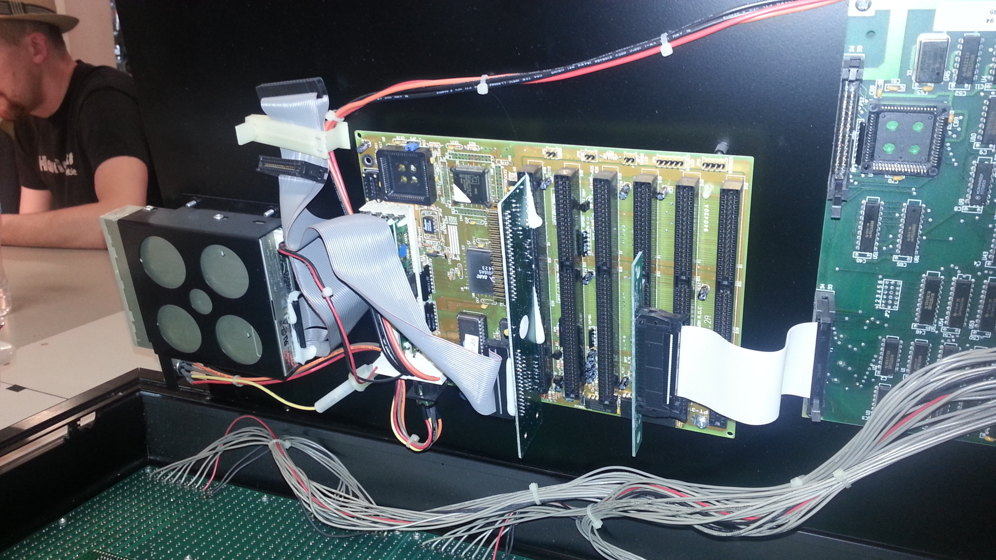
To a board containing a hodge podge of tri-state flip flops, line decoders, latches, and sram, I saw SN74HC574N, MC14514, LH5116-10 . There are also 16 IRFZ40 mosfets. This isn’t a complete list because this was more of a poke about and get a feel for it rather than a full reverse engineer fest.

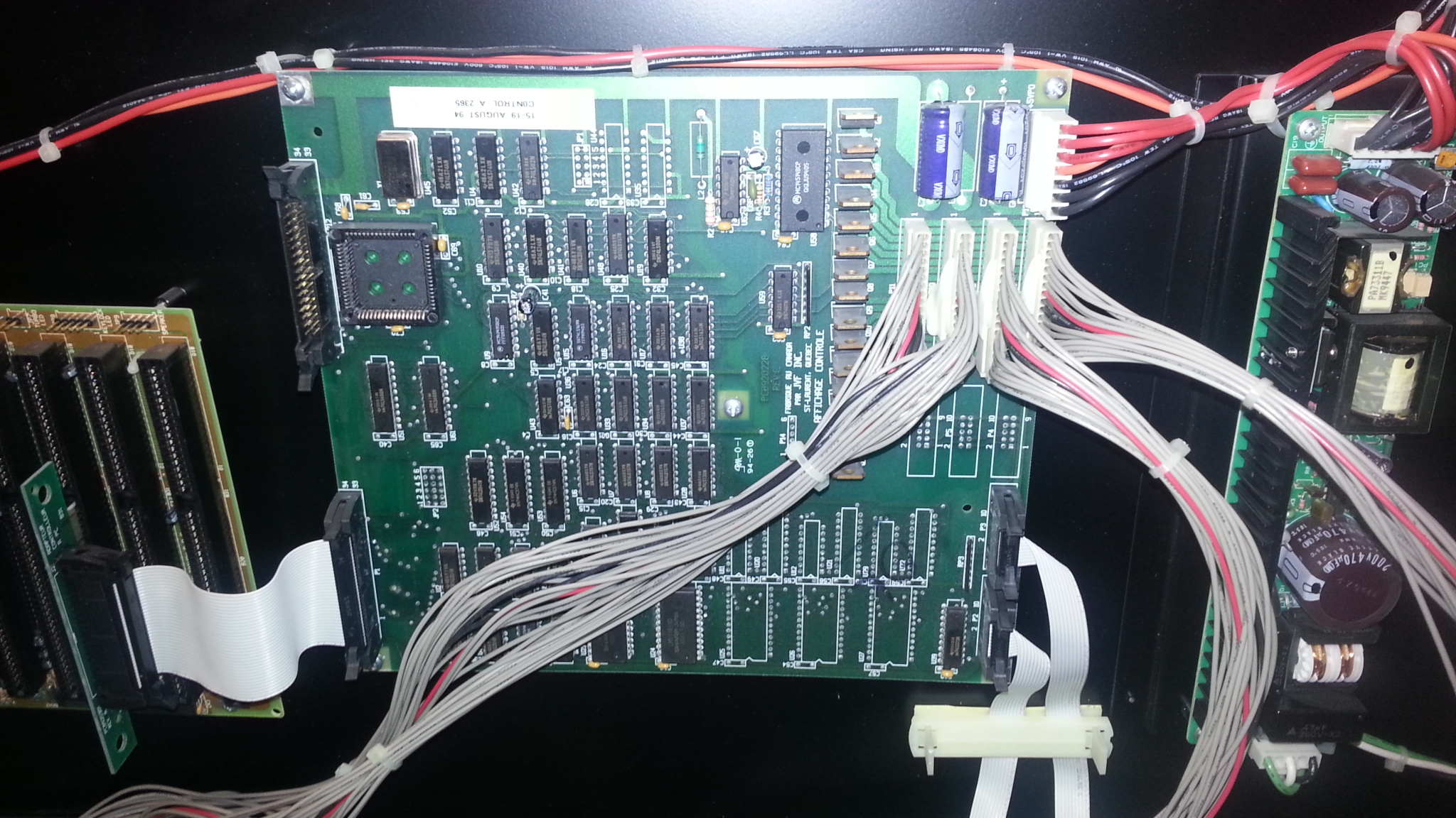
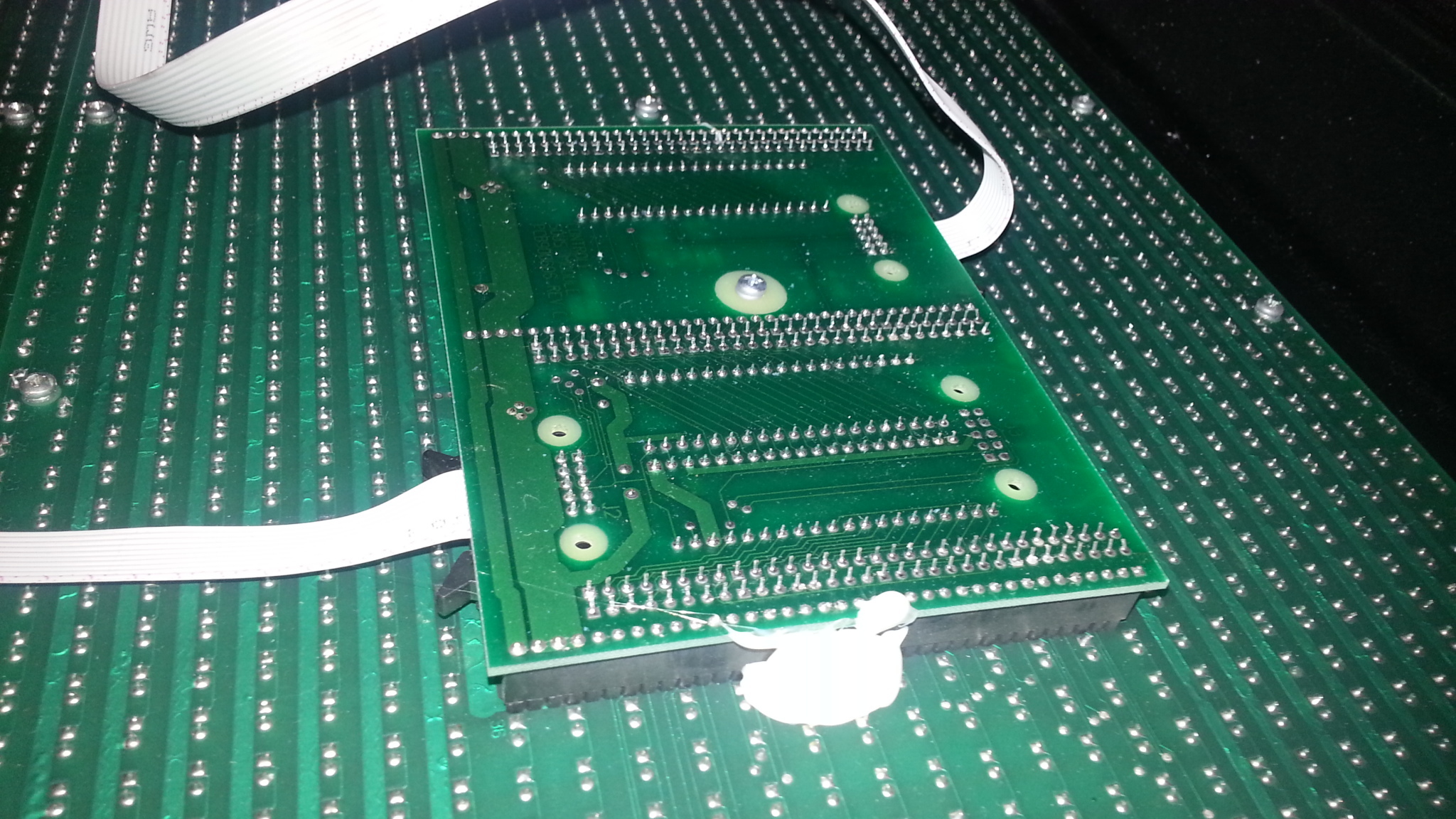
The heavy power cables next to the mosfets go to rails hooked up to the leds (forgot to note it if its common cathode or anode), and there are also 10 connector ribbon cables going to this board which is screwed and glued to the back of the led board:

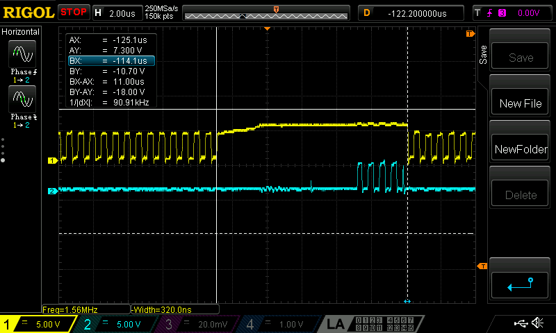
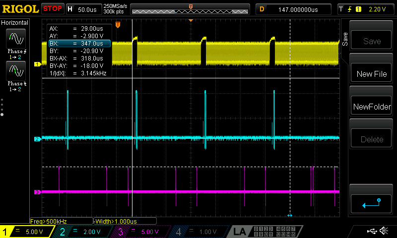
For entertainment, I scoped the first three lines off that 10 conductor ribbon cable (the other 7 appear to be ground, which seems odd, perhaps this is just in their latched state, should recheck this when its powered next time). Not the most useful result but hey this new scope is fun.


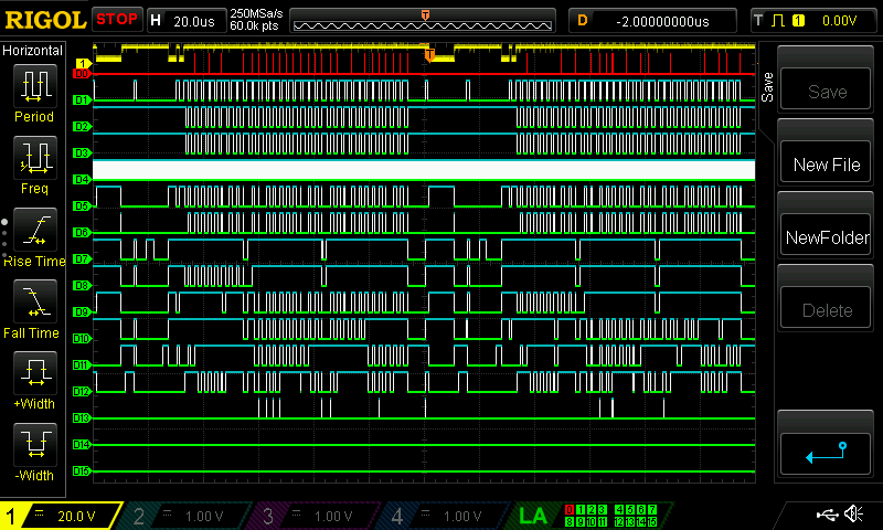
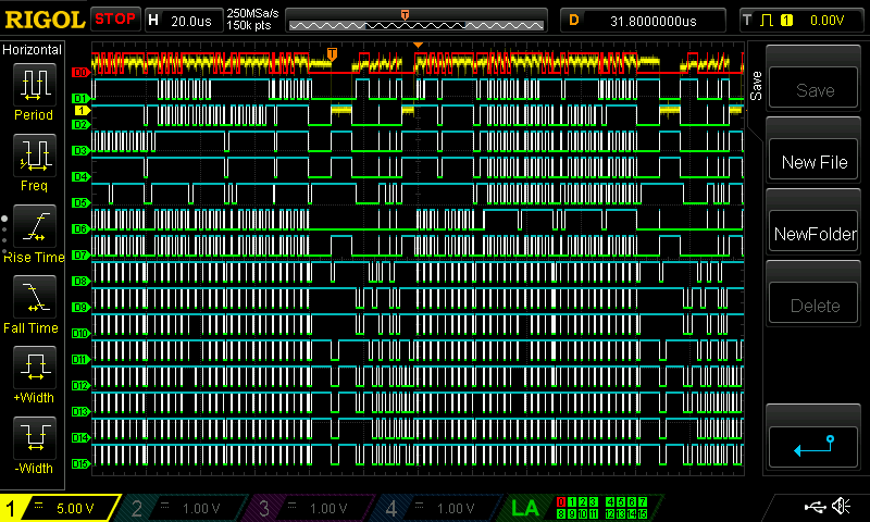
So yeah, I think my plan from here is to hook a logic analyzer up to that main ribbon cable coming off the ISA bus, and see what they protocol is. It might also be worthwhile to spend some time to figure out how they rigged their multiplexing and dimming scheme. It only has 16 mosfets and it seems to be able to individually dim each led (dim into 3 states, on, mid bright and off) so its using some sort of time domain switching.

If anyone has made it this far and has knowledge of how memory registers and flip flops and gates in this era were set up and what is likely to be the control scheme, feel free to chime in, because I have no idea what any of this does and am kinda winging it, or you know, learning.

5 Likes

Nice work.

ISA is pretty slow, could probably bit bang it with an arduino.

Yeah like 8mhz or something, shouldn’t have a problem with any of the AVR’s. A lot of it will depend on how many data lines they are actually using. Be nice to run it off something like an esp8266, not sure if i2c port expanders work on a data bus like that though.

For reference, and for SEO purposes, the LED Sign is a JVF 2010-A. I should also clarify that I misspoke last night; each LED has 4 states: Off, 1/3 brightness, 2/3 brightness, full brightness. Apparently the 2/3 brightness is barely discernible from full brightness.

I looked online a little harder this time and found some more information and pictures of the internals!

John’s Red Sign Page has a good overview of the device and how to operate it the way it was intended, either by preloading images on the floppy disk, or by using a keyboard to program/draw the images.

Noisebridge has photos of the internals, including the daughter boards that we didn’t remove from the back of the LED panels. They have it controlled by an Arduino-compatible, bypassing the 386 motherboard, and supposedly have source code, but the URL is stale and we may need to ask them for it.

mainisusuallyafunction has made some progress reverse engineering the 386 code and writing custom software (GitHub) that plays the Game of Life on the original hardware. It might even be trivial to get this running on our screen, assuming we can find a PC with a floppy drive!

So it looks like we have some options!

4 Likes

That is FANTASTIC shane, thanks for digging those links up. I have edited the title and there goes my morning…
edit : after reading through yup, totally doable, I like the way noisebridge did it, but I am not sure if they are getting the 4 state dimming or not. Something like a teensy 3.1 that has multiple uarts and decent buffering capability should work in place of the two AVR’s they are using.

I have a USB floppy drive ( haven’t used it in years so I’m not sure if it’s still functional )

The GIS PC has a floppy drive, if it hasn’t been replaced. It’s the
one I used to write to the floppy disk in the LED sign in the first
place.

I have a couple that I know work (but no disks). I also bought one of those flash based FDD replacements on ebay, they work well.

Thanks, I will look around! And thanks for writing that original floppy disk so that everyone knows the sign works! I also found that the Sherline CNC mill PC has a floppy drive, but it’s probably not network connected.

So update time, first things first, gotchas:

  1. The power switch on the back switches the neutral not the hot, thus when the sign is pluged in and turned off accidently bridging things to ground is exciting. Keep this in mind when poking around

  2. Most of the custom board has latching flipflops, that latch to ground when its off. This makes it fun to figure out which are actually data lines.

I have worked out most of the pinout on the 386 side and how it maps to the 31 pin ribbon cable to the sign board. Using this and the dos source code from Shanes link you can work out where the dma dumps into the sign. Basically, store all the pixels in memory (2 bits per pixel), dump that via dma to the registers on the custom board in the sign (ribon pins 2-16 I think), and repeat. Should be able to bitbang it as its only going at 2.5mhz or so. Still have to wrap my head around some of the stranger pins and address connections but its solveable.

So far this is my best guess as to the pinout of the ribbon cable between the 386 and the custom board:
format is ribon pin, isa pin, notes.

1 B1 x ?
3 B2 x ?
5 B6 50 khz pulse on startup - nothing on data
7 B1 B3 B10 B31 x ?
9 A11 Base frequency 66.7khz 6mz between data packets 5.8mz of packets 48 separate data groups 2.5ms within data group 1.6 us packets
11 NC x ?
13 B14 x ?
15 b15 high
17 b16 Random short pulses
19 b18 high
21 b17 Random short pulses
23 b20 2.5mhz clock
25 b22 ?
27 a22 ?
29 b26 high
31 nc Random short pulses
33 b31 x
2 A2 Data octal buffer
4 A3 Data octal buffer
6 A4 Data octal buffer
8 A5 Data octal buffer
10 A6 Data octal buffer
12 A7 Data octal buffer
14 A8 Data octal buffer
16 A9 Data octal buffer
18 a23 Data - ISA?
20 a24 Data - ISA?
22 a25 Data - ISA?
24 a26 Data - ISA?
26 a27 Data - ISA?
28 a28 Data - ISA?
30 a29 Data - ISA?
32 a30 Data - ISA?
34 a31 Data - ISA?

Helfpfull stuff is here: jvflife/jvflife.c at master · kmcallister/jvflife · GitHub for the dos code seeing how the DMA transfer is formated and set up

How the ISA dma chip works: Operating Systems Development Series

ISA pinout: Industry Standard Architecture - Wikipedia

3 Likes

So further update, I have now traced all the lines going from the 386 to the logic board. All in all looks like only about 10 pins are relevant, the rest are for enabling floppy access of the board and other such silliness.

Still chunking it through mentally but basically there are a pair of 74ls688n comparitors looking at the address lines, u51 is looking for 11110000 which just happens to be the address (2f0) that is being set in dos when it does the transfer to the sign. U51 output pin19 then enables u52, a 74ls541n which is connected to the data lines coming off the ISA bus.

Short version, looks like I only have to set the address pattern by just tieing the pins high and low, and then dumping the data into u52. So yeah, completely hackable.

Yay! Question: Where is the 2 for the address 2f0? Does DMA only work with a subset of memory, such that DMA can only be done on the 0x200 region of memory? Or does the controller board just not care because it works as is?

No idea, I think they just used it because it was available, those higher bits get basically ignored

From my limited understanding (feel free to correct me) the way the ISA bus works is there are 8 data lines that work in parallel, and 19 address lines. Any transfer on the bus sets the address line for the appropriate destination (or memory address if its connected to the DMA controller at the time), then goes nuts clocking out data (There are also a bunch of IRQ lines and other transfer state lines but they can basically be ignored). The sign is only connected to address lines 2-9 (0 and 1 are connected but go direct to the empty socket for the suspected floppy controller). The address line gets hooked up to a word comparitor, so if it matches the right pattern boom it activates the inputs. There is also a second comparitor but I think its for something else, the output goes towards the socket, TBC.

There is also some weirdness with special bytes being sent via data lines I need to work through and I am not sure how the shift register this is all going into is being clocked (there is an onboard crystal). But I am at the space now working through it.

Step two after I answer the above questions is going to be hooking up a mega to it and having a go. (had this bloody thing in my tool box for 2 or 3 years, might as well use it for something).

So making progress. As a result of tracing back all the logic chips I can make use of the word comparitor to trigger the logic analyzer on the specific relevant traffic for the sign (the ISA bus is connected to EVERYTHING). Pin 19 on u51, set the trigger to pulse. Its the yellow trace at the top of the scope off chanel1.

The first shot is the address lines and misc, the second just the address and data lines. I have better documentation of each in a mess of a spreadsheet but suffice it to say, 32 byte transfers which happens to be width of the sign divided by 4.


Incidentally what I thought was a clock line (the solid white smudge) kind of is, but they are running it through an xor with stuff coming off the AEN and IOR lines to divide the clock frequency down, 1us pulse high and 1us pulse low.

You can also see the preamble data which apparently is important.

Now to replicate this…

1 Like

Ok, so it looks like I am slightly out of the black hole I have been in for the past couple of months…AWESOME!! I actually brought that down to the space and I forgot to bring down the Floppies for it with working animations, if someone wants to decompile the code hit me up on slack.

-Butters

1 Like

Btw 2f0 is Isa I/O port.

There are two address spaces in Isa with separate read and write strobes for each space. I think the I O space is something like 12 bits wide.

Kinda sorta. 2f0 just sets the address lines, there is no I/O port per say as there are only 8 shared data lines
http://www.hardwarebook.info/ISA
Is the best page ive found explaining things. This board runs a little custom and only address bits 0-9 are carried over and only 2-9 are used.

someone beat you to it, from shanes post upthread: main is usually a function: Programming the JVF 2010-A

Im planning on bypassing the 386 and moving the control to a microcontroler which will allow custom rendering and wifi input.

1 Like

We do have a single floppy disk with a simple running animation, so we can at least see it work and probe it in action. :slight_smile:

So I won’t be able to make it down to the space tonight, here are my notes and data sheets, is there a better VHS owned resource I can put this stuff in?

https://www.dropbox.com/sh/akh9dg6hn3nxu5a/AAAA2MStSt5fEHw_Pivz0AQTa?dl=0

the values in the last columns in the sheet correspond to the channels in the LA images above.
Best way to get a stable trace is to connect an analog probe to channel 1 and connect it to pin 19 on u51, set the trigger mode to pulse rising and it works a treat. u51 is a word compairitor sets its output high when the right address is set on the ISA bus. Past that it works best if you connect the logic analyzer probes direct to the chips as indicated in the spread sheet.

General protocol notes, 48 transfers of 32 bytes each. Each corresponding to 1 horizontal row (2 bits per pixel, 128 pixels/4 = 32 bytes). There is some preamble between transfers that I haven’t wrapped my head around, at some point near the very start of the transfer there should be a 0x8F, 0x0F, 0x07, midway though there should also be a 0x05, 0x07 and 0x06, 0x07, all these will be on the data lines.

I haven’t worked out the whole clock yet but so far what I got is that the 2.5mhz system clock seems to be connected to a triple input NAND gate U3 (74ls10n)
pin 3 - goes to u50 (sn74ls08n) pin 10
pin 4 - is the 2.5mhz clock
pin 5 - is connected to ribbon 19 (DRQ1)
pin 6 - the output is connected to U2 (74ls04n) pin 3

So yeah its doing something funky involving DRQ1 that I haven’t figured yet.