https://github.com/MarginallyClever/kicad-ESP8266
KiCAD is a free program for designing PCBs.
In the first part of the program you lay out components and explain to the computer the theory of how your wires will connect the components together. There it does an Electrical Rules Check (ERC) to confirm you haven’t forgotten to power a chip or left a wire unconnected. I’ve made a KiCAD component for the NodeMCU and added it to a fork of jdunmire’s ESP8266 KiCAD models.
In the second part of the program you assign footprints to each component. That means you say “this component has this physical shape on the PCB.” (for any given component there might be dozens of footprints, so choose carefully.) Once you’ve set footprints for each component it’s on to part three, arranging the footprints, drawing the traces (wires), and running a Design Rules Check (DRC) to be sure it seems electrically sound. I’ve made a footprint for the NodeMCU 1.0.
KiCAD is not intuitive in many ways for me. I hope that by making these parts available your life will be made a little easier.
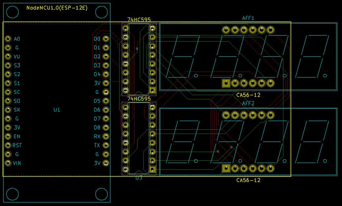
After taking this screenshot I went back and added the USB jack and the Wifi antennae to the footprint for better layout. The circuit above is my home “is vhs open” clock.